Engineering notebook
Modbus Anywhere PCB design
Design notes from turning a Modbus prototype into a DIN-rail PCB that can live in the cabinet instead of dangling from a USB dongle.
- Published
- Projects
- Modbus Anywhere
- Part 1 - PCB design
- Part 2 - Test firmware
- [Part 3 - Real firmware]
Why bother with a custom board?
During the early stages of my house renovation, I have been trying a few different smart home and energy monitoring options before committing to anything more permanent. I already have OpenEnergyMonitor, Home Assistant and a few bits of test hardware on the go, partly to understand what I actually care about and partly to get ready for a future heat pump installation I want to monitor via HeatPumpMonitor.org.
One of the things I wanted to measure was the electricity consumption of a water heater, so I wired in an Eastron SDM120M meter. The standard pattern here is fairly simple: mount the meter in the DIN cabinet, then run a pair of wires from its Modbus terminals over to a USB RS-485 dongle plugged into a Raspberry Pi somewhere nearby.
That works, but it is not especially tidy. It also quietly assumes the Pi has to live close enough to the cabinet for those wires to be practical.
The idea behind Modbus Anywhere was to get rid of that constraint. Instead of a meter in the cabinet and a dongle hanging off a Pi somewhere else, I wanted a small module that could sit in the DIN enclosure itself, talk to the meter over RS-485, and then get the data onto the network over Wi-Fi. That removes the trailing USB cable entirely and means the compute side can live somewhere completely different if that is more convenient.
Turning that into a PCB felt like a sensible next step after proving out the basic RS-485 side of things with a prototype.
The schematic
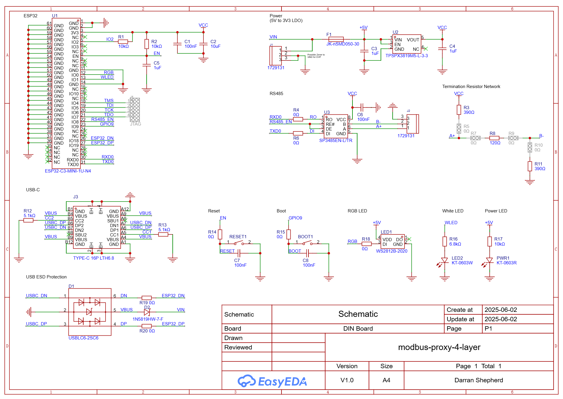
Putting the schematic together was mostly a case of reading datasheets carefully and copying the reference designs with a bit more discipline than I usually manage on a breadboard. The broad shape of the design was not especially exotic: ESP32-C3 module, RS-485 transceiver, power supply, boot and reset buttons, and the supporting passives to make each part behave itself.
The part that took longer than expected was not the topology but the component selection. There are lots of plausible choices for the boring bits such as regulators, and I did not have strong opinions on most of them. My rough heuristic was to favour parts that JLCPCB already held in large quantities. That felt like a reasonable compromise between not overthinking it and avoiding a design that immediately becomes awkward to reorder.
The PCB layout
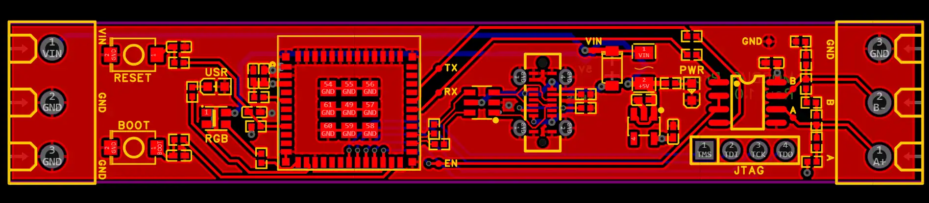
The main physical constraint was the enclosure. I wanted the whole board to fit inside a single-width DIN module, which meant working to roughly 14.5 x 85 mm. That is generous enough for terminal blocks and a small module, but not generous enough to be careless once an ESP32 module, power input and RS-485 interface all need to coexist on the same board.
I started out assuming this should be a two-layer board because that felt simpler and cheaper. In practice that turned out to be false economy. I spent quite a while trying to thread tracks around the ESP32-C3 module and gradually concluded I was mostly optimising for my own misplaced sense that four layers was somehow extravagant.
Once I switched to a four-layer stack-up and gave myself internal 3V3 and GND planes, the routing became much more straightforward. I would probably start there next time rather than trying to force a two-layer solution out of stubbornness.
Getting boards made
I used EasyEDA for this board. Partly that was because the web-based workflow lowered the barrier to entry a bit, and partly because the path from finished design to a JLCPCB order is about as short as it could realistically be.
On that front, it did exactly what it promised. Once I was happy enough with the layout, exporting the manufacturing data and turning it into a populated board order was almost suspiciously easy. A few clicks later the order was placed and I spent the next several days checking the status page far more often than was necessary.
Just over a week later, five assembled boards arrived.
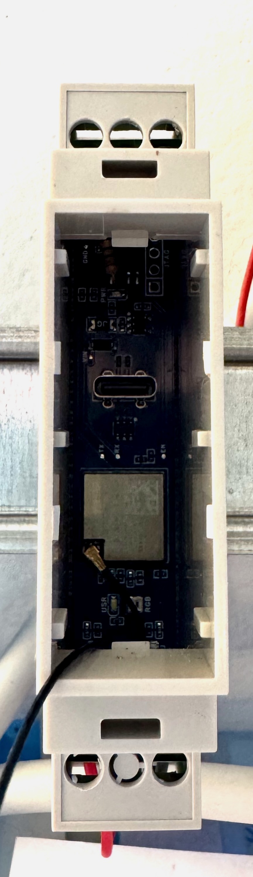
First power-up
This is the bit where the story stopped being quite so tidy.
Flashing test firmware onto the first board was unreliable. Sometimes it would program happily, sometimes it would refuse to boot in a useful way, which is not the sort of uncertainty I was hoping to discover at this stage. After a bit of poking around, I realised I had made a poor choice of pin for the RS-485 transceiver direction control.
I had used IO8 as the transceiver enable signal, which clashes with its role as a strapping pin during boot. My mistaken reading of the datasheet was that because the pin’s default state was floating, it would not matter much what was hanging off it. That was too casual. In the finished board, that connection was enough to interfere with reliable startup.
Thankfully the fix on these first boards was not too horrible. The transceiver is in an SOIC-8 package, so I could bodge in a 10k pull-up resistor between its enable pin and 3V3 and get the board into a much happier state.
The second problem was more embarrassing because it was entirely self-inflicted. While copying the reference design from the ESP32-C3-MINI dev kit, I missed that the debounce capacitors on the boot and reset buttons were marked NC, meaning the footprints exist but the parts are not intended to be fitted. I populated them anyway.
That turns out to be a neat way to create an RC delay on the ESP32 enable pin and stop the module booting normally on first power-up. Once the board had power, pressing reset would bring it to life immediately, which was a useful clue, but not one I would have preferred to need.
What I would change in the next revision
The encouraging part is that both faults are easy to explain and easy to fix in the next board revision.
- Add a 10k pull-up to the IO8 strapping pin, or move the RS-485 direction control to a different IO pin.
- Do not populate the boot and reset debounce capacitors.
- Keep the general board shape and enclosure approach, because that part worked as intended.
So although this first spin was not quite the clean success story I had in mind, it did prove the important bit: I can get the whole interface onto a compact board that fits in the DIN cabinet, without needing a USB dongle and a trailing pair of wires back to a nearby Pi.
The next step from here was to get some deliberately simple firmware onto the board and prove out the basics of UART, RS-485 direction control and talking to the SDM120 reliably. That will be the next part in this little mini-series.